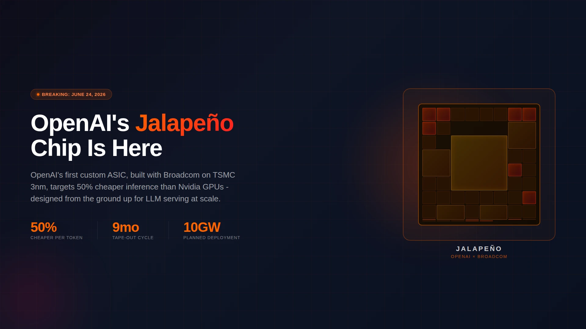
On June 24, OpenAI and Broadcom announced Jalapeño - OpenAI’s first custom AI accelerator. It’s a reticle-sized ASIC manufactured at TSMC 3nm, designed from scratch for LLM inference, and aimed at cutting OpenAI’s inference compute costs roughly in half compared to current Nvidia GPUs.
This is not a press-release chip. Engineering samples are already running ML workloads in the lab. Microsoft is reportedly lined up to buy around 40% of the initial production run for Azure. The companies have committed to deploying 10 gigawatts of these accelerators between late 2026 and 2029.
Summary
- Jalapeño is OpenAI’s first custom inference ASIC, co-developed with Broadcom, manufactured at TSMC 3nm.
- The chip targets ~50% lower cost per inference token vs current Nvidia GPUs, with comparable performance to Blackwell.
- It went from initial design to manufacturing tape-out in nine months - reportedly the fastest ASIC development cycle ever for high-performance advanced semiconductors.
- Prototype deployments begin late 2026, full ramp in 2027-2028. Microsoft is slated to absorb ~40% of initial production.
- No immediate API changes for developers. The payoff is cheaper API prices and faster responses - eventually.
- OpenAI joins Google (TPUs), Amazon (Trainium/Inferentia), and Apple in building away from single-supplier dependence on Nvidia.
What Jalapeño actually is
Jalapeño is an inference ASIC. Not a GPU. Not a training chip. Not a general-purpose compute device.
The architecture centers on a systolic array - a grid of processing elements that pass data from cell to cell in rhythmic lockstep. That pattern is ideal for the dense matrix multiplications that dominate LLM inference. Surrounding the compute die are eight HBM stacks arranged on a silicon interposer in 2.5D packaging. The goal of that layout is to minimize the distance electrons travel between memory and compute, which is where most inference latency hides.
The die is reticle-sized, meaning it’s the largest die TSMC’s lithography can expose in a single shot on a 300mm wafer. Every millimeter of silicon goes to either compute or memory bandwidth, because that’s what LLM serving needs. There’s no gaming engine. No video decode block. No general-purpose FP64 units that serve nothing in an LLM serving stack.
Broadcom designed and implemented the silicon. Celestica is the ODM - they handle boards, rack systems, thermal management, and production-scale manufacturing pipelines. OpenAI’s own models reportedly accelerated parts of the chip design process itself, which is a detail the announcement mentions but doesn’t quantify.
The unit economics argument
Before getting into comparisons, it helps to understand why inference-specific silicon makes sense at all.
Nvidia’s H100 and Blackwell GPUs are excellent general-purpose accelerators. They can train models, run inference, simulate physics, render scenes, and do scientific computing. That flexibility is genuinely useful when you’re a hyperscaler with diverse workloads. But for pure LLM serving, you pay a real price for it in power consumption and silicon area that isn’t doing anything for your chatbot.
LLM inference is an unusually homogeneous workload. The operations - attention, linear projections, softmax, sampling - repeat across every token, every request, every model in the same broad family. The memory access patterns are predictable. The compute graph doesn’t change. An ASIC designed around those patterns can shed the generalist overhead and run more inference per watt per dollar.
Google validated this with TPUs in 2016. Amazon ran the same playbook with Trainium for training and Inferentia for inference. Apple builds Neural Engines for on-device ML. The concept is proven. OpenAI is late to it, not pioneering it - but the scale they’re proposing is notable.
OpenAI reportedly spent around 50% of its revenue on inference compute costs in 2025. At the volumes they’re running - ChatGPT, Codex, API traffic - even a 20% improvement in cost per token translates to hundreds of millions of dollars annually. A 50% reduction is a structural change to the business.
How it compares to Nvidia
The honest answer is that nobody outside OpenAI and Broadcom knows exactly how Jalapeño performs on real workloads, because no independent benchmarks have been published.
What Broadcom CEO Hock Tan has said is that Jalapeño delivers performance “on par with Nvidia’s Blackwell generation” - the current generation H200 and B100/B200 family. The 50% cost figure refers to cost per inference token, not raw FLOPs. Those are vendor-reported numbers from early lab testing, and they should be treated as such until there’s an independent MLPerf result or equivalent.
The comparison that matters isn’t peak TFLOPS - it’s cost to serve a million tokens in production. A chip that does inference at half the dollar cost per token is straightforwardly better for this use case even if it loses on a synthetic peak-throughput benchmark, because inference is priced per token, not per FLOP.
Nvidia’s H200 has a list price around $35,000-40,000 per GPU. The Blackwell B200 SXM runs higher. Those numbers don’t include the rack, networking, power, cooling, and OpEx to keep them running. OpenAI hasn’t published Jalapeño pricing, but the claim is that the fully-loaded cost-per-token comes out around half of what current GPU infrastructure delivers.
Nvidia’s response to this is straightforward: they keep shipping faster chips. The H200 improves on the H100, the B200 improves on the H200, and the Rubin generation is already in planning. For a company buying 40,000 GPUs at a time and upgrading every 18 months, the absolute edge still matters. But OpenAI isn’t buying chips - they’re building the infrastructure layer they operate on, and a purpose-built chip lets them amortize the design cost across a longer deployment cycle.
The silicon war context
Every major hyperscaler is now building custom silicon for AI. This is not a coincidence.
Google’s TPU v5 runs Gemini inference internally. Amazon’s Trainium 2 and Inferentia 3 are in production for AWS customers. Microsoft has its own Maia 100 chip for Azure workloads. Apple’s M-series silicon offloads ML inference to the Neural Engine on every Mac. Meta’s MTIA runs recommendation models at scale.
The pattern is consistent: at large enough volume, building your own chip beats buying Nvidia’s. The crossover point depends on how homogeneous your workload is and whether you can commit to the engineering and capital required to design and tape out custom silicon. For model-scale AI inference serving, every frontier lab has now concluded it’s worth it.
Nvidia’s advantage has been that they were years ahead and their software ecosystem - CUDA, cuDNN, TensorRT - is deeply embedded in every ML workflow. That ecosystem moat is real and doesn’t disappear because OpenAI released a chip. But the hardware moat erodes every year as more silicon alternatives prove out on real inference workloads.
What actually changes the economics for Nvidia long-term is not one competitor chip - it’s the combined signal that their pricing power for inference is structurally limited. When Google, Amazon, Microsoft, and OpenAI all have their own inference silicon in production, Nvidia’s ability to charge a premium for the H-series and Blackwell line gets tested every contract renewal cycle.
What this means for developers now
Directly, nothing changes today.
If you call the OpenAI API, you get responses served on whatever hardware OpenAI runs today. There’s no Jalapeño configuration flag, no model suffix indicating you’re on the new chip, no latency difference you’d notice. The chip isn’t in production yet.
What developers should watch:
- API pricing over the next 18 months. If Jalapeño delivers on its cost promises, OpenAI has room to cut token prices while maintaining margins. They’ve already cut API prices significantly since 2023. Cheaper inference economics accelerate that trend.
- Context window and throughput improvements. Larger HBM capacity per chip means the chip can hold bigger KV caches in memory. That matters for long-context requests where the bottleneck is memory bandwidth and capacity, not compute.
- Availability at peak demand. One reason API reliability degrades during high-demand periods is that Nvidia GPU supply is constrained and expensive. A chip supply chain OpenAI controls directly should reduce those bottlenecks.
For applications that are currently too expensive to run at scale - high-frequency agentic workflows, large context document processing, real-time AI features - cheaper inference arithmetic is what unlocks them commercially. Not because the model gets smarter, but because the cost-per-query drops to a level where the unit economics work.
What’s still unclear
Nine months to tape-out is genuinely fast. Too fast, skeptics would say, for a chip optimized enough to beat Nvidia’s efficiency at inference. The counterargument is that OpenAI has an unusually detailed understanding of their inference workloads, which lets them design a chip that’s optimal for a narrow target rather than a general one. That’s plausible. It’s also the kind of thing that only shows up in production benchmarks.
The big unknown is software. CUDA’s dominance isn’t just the hardware - it’s the millions of lines of kernels, the profiling tools, the debugging support, and the institutional knowledge that every ML team has built around it. Custom ASIC silicon requires its own compiler toolchain, its own kernel library, its own operator support. Google has spent a decade building XLA and JAX around TPUs. Amazon has Neuron SDK. OpenAI would need equivalent tooling for Jalapeño, and none of that was announced.
Broadcom is the silicon partner, not the software partner. If OpenAI is running their own serving stack - which they are - they control the software layer already. But that’s different from providing a chip that external developers can target. Jalapeño is almost certainly infrastructure-internal to OpenAI’s serving stack, not a chip you’ll buy from AWS or run on your own machines.
The deployment reality
- Late 2026: Prototype deployment in lab environments, small-scale testing.
- 2027: Full production ramp begins. Microsoft starts taking delivery of the ~40% it’s reportedly purchasing.
- H1 2028: Peak volume deployment across gigawatt-scale data centers.
The 10 GW figure across the 2026-2029 window is the ambition. That’s not 10 GW of Jalapeño alone - it’s 10 GW of combined custom accelerator capacity across the OpenAI-Broadcom-Celestica-Microsoft partnership. To put it in perspective, a large-scale Nvidia GPU cluster runs on the order of 10-100 MW. 10 GW is two orders of magnitude larger in aggregate.
Whether that scale materializes depends on how well Jalapeño performs in production, whether OpenAI’s revenue trajectory can sustain the capital expenditure, and whether Microsoft and other infrastructure partners remain committed. Those are real questions. But the chip exists, it’s running workloads in the lab, and the partnerships behind it are serious.
OpenAI has been spending roughly half its revenue on compute costs. Building the chip layer is a reasonable response to that. Whether Jalapeño delivers on its promises depends on production benchmarks nobody outside the companies has seen. But the direction is clear: the era of “rent Nvidia GPUs and serve your model on them” is moving toward “run your own inference stack on hardware you designed.” Every company with enough volume is following the same path. OpenAI is following it too.
The practical effect for developers is that inference gets cheaper over time. That’s been true for three years and Jalapeño is another mechanism making it truer. The question is just the pace.